Control Systems Used For Semiconductor Wafer Polishing
How are silicon wafers polished?
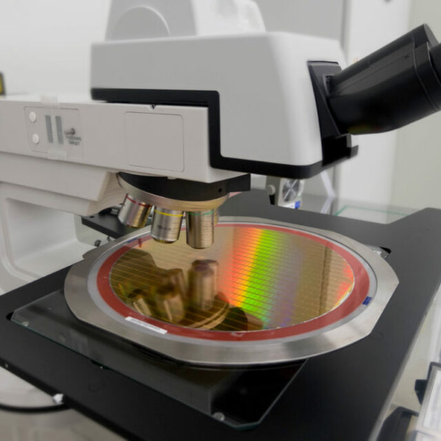
Silicon wafers are polished to create a flat, smooth surface that is essential for semiconductor manufacturing. Polishing removes any irregularities from the wafer surface and helps to create a mirror-like finish. There are two main types of polishing: chemical-mechanical polishing (CMP) and physical vapor deposition (PVD). CMP involves using a chemical solution to remove material from the surface of the wafer, while PVD uses a physical process to deposit thin films onto the wafer surface. Silicon wafers are typically polished using CMP, as this method can achieve a higher degree of accuracy and precision.
Chemical Mechanical Polishing (CMP)
Chemical Mechanical Wafer Polishing is a process that uses a combination of chemicals and mechanical polishing to remove material from the surface of a semiconductor wafer. The chemical component of CMP reacts with the surface being polished, while the mechanical component removes material through physical abrasion. CMP is a highly controlled process, and variations in the composition of the chemical solution and the type of polishing pad can result in different rates of material removal. In addition, CPA can be used to clean semiconductor surfaces by removing particles that could otherwise cause defects in the finished product.
This process can be used to achieve precise thickness control and flatness for subsequent processes, such as lithography and deposition. Pressure regulating chemical mechanical wafer polishing helps to ensure consistent results by controlling the pressure applied to the wafer during the polishing process. This helps to avoid problems such as warping or uneven polishing. In addition, pressure regulating chemical mechanical wafer polishing can also improve the quality of your finished product by minimizing defects on the surface of the wafer. By understanding how this process works, you can better optimize your own manufacturing processes using chemical mechanical wafer polishing techniques.
Chemical Mechanical Polishing Vs Planarization
A chemical-mechanical polishing procedure, CMP, removes surfaces by means of chemical reactions and is often associated with chemical-mechanical planarization. The Chip Manufacturing Process is a standard manufacturing process used in manufacturing integrated circuits and memory disks in the semiconductor industry. A chemical-mechanical polishing process is used to remove surface materials. Chemical-mechanical planarization, on the other hand, is used when the goal is to flatten a surface. Because friction and corrosion are synergistic in CMP, it is classified as a tribochemical process.
Chemical mechanical polishing (CMP) and Chemical Mechanical Planarization (CMPA) are both widely used semiconductor fabrication processes. In CMP, the semiconductor wafer is polished using an abrasive pad in conjunction with a chemical slurry. The goal of CMP is to remove material from the surface of the wafer in order to achieve a specified level of surface finish. CMPA, on the other hand, is primarily used to planarize the surface of the wafer, meaning that it is flattened out. Unlike CMP, which removes material from the surface of the wafer, CMPA adds material to the surface in order to achieve planarity. As a result, CMPA is a much slower process than CMP.
Pressure Regulation In The CMP Process
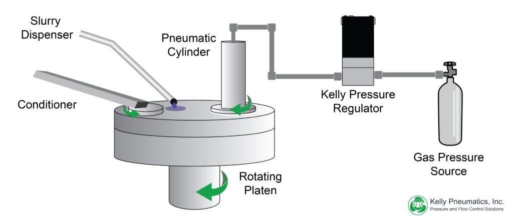
In semiconductor manufacturing, chemical mechanical polishing (CMP) is a critical process for creating smooth, flat surfaces on semiconductor wafers. The pressure at which the CMP process is performed is a critical factor in determining the quality of the finished product. If the pressure is too high, it can damage the semiconductor material. If the pressure is too low, it can result in an uneven surface. A pressure regulator is a device that controls the pressure in a CMP system, ensuring that it remains within a safe range. By keeping the pressure within a safe range, the pressure regulator helps to ensure that the semiconductor wafers are not damaged during the CMP process.

Using the Kelly Electronic Pressure Regulator In The CMP Process
The Kelly Low Flow Regulator is an excellent solution for using precision pressure control to pilot operate the pressure applied to the wafer during the polishing process. Since the regulator is electronically controlled, it can be programmed dynamically by a control system, such as a PLC. This means it can be customized to accurately vary the pressure applied depending on the particular wafer being polished. This provides software engineers the option to preset the regulator to the required pad pressure per CMP sequence. Also, since the pressure regulator is closed-loop controlled, the pressure applied to the polishing pad is maintained even during changes to the downstream pressure, meaning manual adjustment is not necessary.
The regulator also has a feedback signal (analog voltage) representing the current downstream pressure, which can be recorded during the CMP process. This allows for real-time logging of the actual pressures applied through the entire operation, which can be read from the feedback signal into the controller via an ADC (Analog-to-digital converter) and reviewed at a later time. Logging actual CMP pressures applied during the polishing process can provide much-needed traceability for large-scale CMP operations.
What Kinds of Valves are used in the CMP Process?
CMP is performed using a rotating polishing pad and a chemical slurry. The polishing pad removes material from the wafer surface, while the slurry helps to lubricate the pad and remove debris generated by the polishing process. CMP can be performed using different types of pads and slurries, depending on the type of semiconductor material being processed. Different types of valves are used to control the flow of slurry during CMP, including solenoid valves, proportional valves, and ball valves. Each type of valve has its own advantages and disadvantages, so it is important to select the valve that best meets the needs of the particular application.


